

Welcome to Day 3 of the biggest AI conference of the year. NVIDIA’s GTC is going in full swing and we are bringing the best of GTC to you. As always, we recommend you register for free and attend the conference yourself and stand a chance to win RTX 4080 GPU!

In the first 2 days of GTC, we saw many amazing talks on transformers, MLOps, Robotics, cloud computing, computational lithography, and Omniverse to name a few. If you aren’t up to speed with those, please take a look at our summary of the first two days here
- Day 1 Highlights: Welcome to the future!
- Day 2 Highlights: Jensen’s keynote & the iPhone moment of AI is here!
Let’s look at some of the most interesting talks on Day 3 of GTC.
Table of Contents
- FP8 for Deep Learning [S52166]
- Accelerating Computational Lithography [S52510]
- Advances in Operations Optimization [S52063]
- 43% speedups with PyTorch 2.0 [S52422]
- EUV Mask Inspection with AI [S51041]
- GPU accelerated circuit simulation [S51040]
- Summary
FP8 for Deep Learning [S52166]
FP8 is one of the next leaps in deep learning toolkit that all engineers and students should be aware of. FP8 refers to a new data format consisting of 8-bit floating point operations. Introduced in the Hopper architecture, FP8 offers double the computational throughput of half precision fp16 computations as well as significantly increased memory transactions. This offers tremendous benefits for training and inference of deep neural networks, particularly transformers. Here are a few key takeaways from this talk:
- As a recap, we mention that Tensor Cores are specialized hardware units in NVIDIA GPUs which accelerate FMA operations for deep learning. Tensor Cores are anywhere from 8-64x faster than naive CUDA based matmul operations.
- There are 2 types of FP8 standards, one with 5 exponent and 2 mantissa bits, called E5M2 and another with 4 exponents and 3 mantissa bits called E4M3. One bit is always reserved for ‘sign’.
- Hopper Tensor Cores support quarter-precision matrix multiplies for training deep learning models.
- One of the advantages of training in FP8 is that there is no additional step required for post training quantization. Since the model is trained in FP8, it can be directly used for inference at the same precision as training time, which means that there is absolutely no performance degradation during inference.
- FP8 training works for a variety of model architectures like CNNs and transformers. Further, within computer vision, FP8 has been successfully used for training all kinds of models for image classification, detection, segmentation, etc.
- FP8 is available if you are programming directly in CUDA as well as in deep learning frameworks like PyTorch or JAX via the open-source TransformerEngine library, maintained here.
- No hyperparameter change is required between fp18 and fp8 training!
If you would like some background on the concepts mentioned here, please take a look at this blog post where we describe FP8 in more detail.
Demystifying GPU architectures for Deep Learning
Accelerating Computational Lithography [S52510]
In this talk, NVIDIA’s VP of Advanced Technology Group, Vivek Singh shared the technical details behind the Computational Lithography announcement we saw in Jensen’s keynote yesterday. To recap, NVIDIA has developed a CUDA library called cuLitho to accelerate computational lithography by orders of magnitude over previous CPU based approaches. This work was done jointly with TSMC, ASML and Synopsys.
Coming to the technical details, Vivek first explained the physics behind lithography. When light falls on a photomask, it undergoes diffraction following the famous Maxwell’s laws of electromagnetism, compactly represented by the four equations shown in the figure.
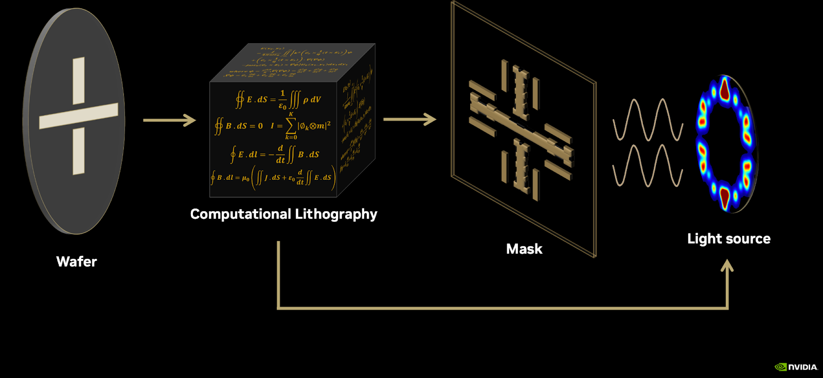
These are non-linear and coupled partial differential equations whose boundary conditions are specified by the mask pattern. As you can imagine with anything physics and PDEs, approximations go a long way in solving them for most practical cases. In fact, this is precisely what the chip industry has been doing for the last 20 years!

As shown in the figure above, up until the 1990s, the features in transistors were so large that diffraction wasn’t a concern and you could design a mask pattern to be exactly the shape you wanted to be printed on a silicon wafer. Around the turn of the millennium, the features became small enough that optical proximity correction (OPC) began to be applied. As shown in the figure, the above ‘+’ shaped figure required corrections in the form of basic ‘dog ears’ shape. These can be thought of as first order terms in a Taylor series approximation.
As the features kept getting smaller and smaller, more and more terms were added until we ended up with a fully analytically correct solution with many terms, as shown in the right hand side of the figure. This fully analytical solution is called Inverse Lithography or ILT. However, ILT poses a very difficult computational problem which is currently solved by clusters of CPUs in dedicated datacenters.
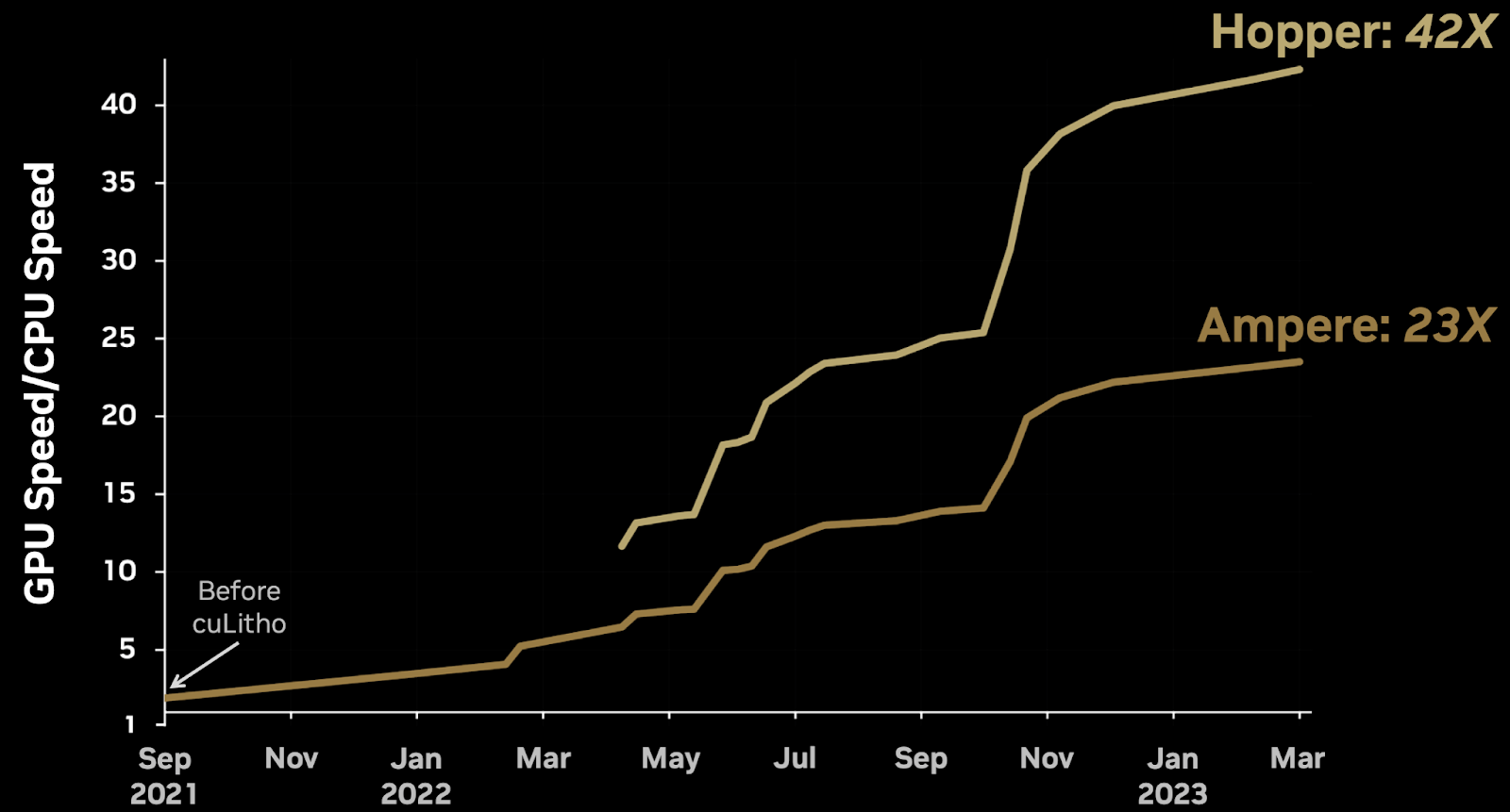
The breakthrough comes in the form of cuLitho, a CUDA based library to accelerate ILT calculations. Vivek shared that behind the scenes, their teams have been hard at work optimizing and improving cuLitho. As shown in the figure, they observed step function-like improvements using cuLitho which accumulated over time until they ended up with 42x improvement compared to CPU processing. Notably, this speedup is for OPC on the entire reticle, as opposed to a small region. This means that cuLitho can be used by foundries right away as a mature alternative to CPU based ILT.
Finally, as a visual example to showcase the kind of complexity cuLitho enables, here is a very complex pattern. Can you guess what it will print?
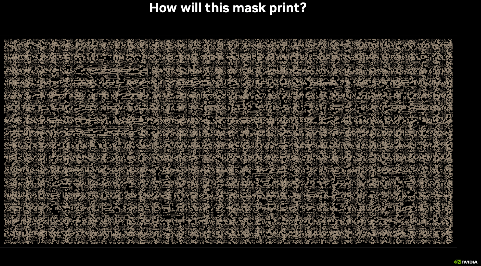
Well, the above is quite non intuitive but it prints NVIDIA’s logo and the word ‘cuLITHO’, as shown below.

All the figures in this section are courtesy of NVIDIA.
Advances in Operations Optimization [S52063]
Warehouses are the beating hearts of the global supply chains. This talk provided a case study of how several NVIDIA tools are helping Pepsico optimize their operations. The daily operations in a warehouse consist of five basic tasks:
- Receiving goods
- Put away
- Storage
- Picking
- Shipping
The three key parameters that drive cost are: Labor, Space and Equipment. In this case study, we take the example of decanting and picking stations. The objective here was to develop an accurate digital twin representation of the station. The twin would enable high accurate perception solutions for video analytics. Finally, the third objective was to optimize the operations using several different simulated strategies. The following NVIDIA tools were helpful in this project:
- Omniverse was used to create USD models of various different assets in the warehouse. This allowed synthetic data generation for training of perception pipelines.
- The Metropolis Microservices Platform enabled streaming of sensor data into Intelligent Video Applications (IVAs).
- TAO toolkit was used to quickly train perception models.
- DeepStream was used to create efficient IVA inference pipelines.
Although the presenters did not share any concrete numbers about the difference in cost or other KPIs as a result of this project, the conclusion was clear. Pepsico believes that creating digital twins with the tools mentioned above would allow them to simulate various scenarios and optimize their operations.
43% speedups with PyTorch 2.0 [S52422]
PyTorch is one of the most popular frameworks for development of machine learning models. This talk covered some of the major features of the new PyTorch 2.0 release. The key observation behind this project is that we are increasingly bound by memory rather than compute. For example, from V100 to A100, memory bandwidth increased only by 1.7x while compute capabilities increased by ~5x. The PyTorch team needed a plan to improve performance and they came up with 4 broad requirements that PyTorch 2.0 should fulfill:
- First, for the ML practitioner, there should be at least 30% speed ups and lower memory usage with no modifications to the code.
- Second, a hardware engineer should find it substantially easier to write a backend for PyTorch for their custom accelerator.
- Third, the distributed compute abilities of PyTorch 2.0 should be state of the art, and finally
- As much as possible, PyTorch 2,0 should be written in Python, so that it is substantially easier for others to contribute to the source code.
To achieve these goals, the team made some amazing breakthroughs:
- TorchDynamo is a graph acquisition tool that acquires the computational graph of the entire model when you call torch.compile(model). torch.compile is a new function available in PyTorch 2.0 and just by adding this one single line of code, you can experience ~43% higher training performance (43% is the geomean across a range of representative models, your mileage may vary). If however, you do not add the torch.compile line to your code, nothing bad will happen. Your code from PyTorch 1.x remains fully compatible with PyTorch 2.0.
- The team has significantly reduced the number of operators required for implementing all PyTorch functions from >2000 down to just around 250. This significantly speeds up development of custom backends for PyTorch (typically by companies like GraphCore and Habana Labs, which develop their own training chips).
- TorchInductor is the compiler that compiles the acquired and lowered graph. The key thing to note is that TorchInductor is powered by OpenAI’s Triton backend rather than cuDNN. This means that as of the time of writing, CUDA acceleration for PyTorch 2.0 is supported for Volta and Ampere generation GPUs, but Pascal and older architecture are not supported. Active work is going on to extend support for older GPUs.
EUV Mask Inspection with AI [S51041]
In this talk, Sagar Trivedi from TSMC presented some impressive advances in using AI to inspect EUV masks for defects. Extreme Ultraviolet (EUV) lithography is the latest chip manufacturing technology that is driving the semiconductor industry forward due to its very high precision. However, with very high precision also comes the chances of high defects in the photomask. There are three major challenges faced by TSMC in mask inspection:
First, the size of the data is extremely large. A photomask or reticle is only 26 mm x 33 mm, or not much bigger than the size of a fingernail. So how big could an image of that size be? Well, it turns out pretty big if your resolution is 5 nanometers, which is 20,000 times smaller than the width of human hair!!
According to the numbers shared by TSMC, a single reticle (photomask) image is ~35 TB. A single chip like H100 uses ~70 or so reticles. This would mean that the images of one set of H100 reticles would be about 2.45 petabytes!! Since H100 is just one of the many chips that TSMC manufactures, we can see that the size of the images is absolutely enormous and unmanageable. For each mask to be inspected in a reasonable amount of time, the defect inspection rate should be at least 5 GB/sec.
The second challenge is that the images we obtain from mask inspection tools are not exactly the same as the pattern printed onto silicon wafers. Specifically, actinic inspection tools (actinic just means that the imaging wavelength is the same as EUV wavelength of ~13.5 nm), provide images with ~500x magnification while the scanner optics (aka the pattern printed on silicon) have a 4x reduction. The highly detailed images provided by actinic inspection tools allow identification of even some buried/hidden defects in EUV masks, but this high resolution here poses a challenge for automated mask inspection.
Third and finally, the classical physics based modeling pipeline for EUV lithography consists of several blocks each of which has to be calibrated independently. This is a slow process which becomes a bottleneck.
To solve these challenges, the team created an ML based simulator which is very fast and can keep up with the demands of the 5 GB/sec data processing requirement. Further, the comparison is also GPU accelerated and uses a combination of TensorFlow and TensorRT. This way, the team was able to achieve the required data processing rate of 5 GB/sec with a computational budget of 40 A100 GPUs and 320 CPU cores. We are not adding screenshots of slides from the talk as TSMC is usually extremely secretive about their research, so we highly recommend you to check out the slides by searching the presentation code S51041 in the GTC portal.
GPU accelerated circuit simulation [S51040]
Synopsys is the largest vendor of Electronic Design Automation (EDA) tools. These are basically CAD software used by the semiconductor industry to design their latest chips. As Moore’s law is slowing down, there is demand for adding complexity to chip designs via heterogeneous compute and memory architectures. This makes accurately simulating circuit designs even more important. Any defects captured in simulation are very easy to fix but once a chip goes into production, it can cost millions of dollars and multiple quarters to fix these issues.
This talk was given by Synopsys to demonstrate the capabilities of their state of the art GPU based circuit simulator called PrimeSim. PrimeSim uses several CUDA libraries under the hood like cuSolver, cuBLAS to enable extremely fast circuit simulations. With this capability, PrimeSim was able to accurately simulate power delivery networks (PDNs) in micron memory chips. The simulation time was brought down from 29 days to just 44 hours, a speedup of 15x!
Summary
In today’s post, we have touched upon several topics from FP8 training, PyTorch 2.0, EUV Mask inspection to computational lithography and operations management. We hope you like the semiconductor focus of this post. The semiconductor industry is unique in that it is at the core of most other industries.
The excellent breadth of talks about the impact of AI on the semiconductor industry is unparalleled and such deep talks are difficult to find even in dedicated conferences by IEEE or SPIE. The key takeaway is that AI algorithms and GPU chips are feeding back into their origins, which is the semiconductor industry. They are helping us manufacture more advanced chips which will in turn solve even more challenges, resulting in a multiplier effect that could revolutionize every industry on our planet. It can be very difficult to keep up with these advances and we hope our blog posts are helping you with that.
Please join us tomorrow for a grand finish to this edition of GTC. See you there 🙂