• Home
  • >
  • GPUs
  • >
  • Inside the GPU: A Comprehensive Guide to Modern Graphics Architecture

Inside the GPU: A Comprehensive Guide to Modern Graphics Architecture

Explore the modern GPU architecture, from transistor-level design and memory hierarchies to parallel compute models and real-world GPU workloads.

In computing, Graphics Processing Units (GPUs) have transcended their original role, rendering simple polygons to become the workhorses behind realistic gaming worlds, machine learning advancements, and large-scale scientific simulations. A modern high-end GPU can perform tens of trillions of arithmetic operations every second, a level of performance that once required entire supercomputers.

In this blog post, we’ll walk you through every layer of the RTX 3090 GPU’s Ampere architecture and explain how engineers harness massive parallelism, specialized memory systems, and hierarchical designs to deliver astonishing computational power.

  1. The Exponential Growth of GPU Compute
  2. CPU vs. GPU: Contrasting Design Philosophies
  3. Physical Architecture of a Modern GPU (GA102 Example)
    1. Billion-Transistor Die
    2. Hierarchical Compute Blocks
    3. Microscopic View: Inside a CUDA Core
    4. Memory Controllers, Caches & I/O
    5. Power Delivery & Thermal Management
  4. Binning: One Die, Multiple Products
  5. Feeding the Beasts: Graphics Memory (GDDR6X, GDDR7, and HBM)
    1. GDDR6X SDRAM
    2. GDDR7 SDRAM
    3. High-Bandwidth Memory (HBM3E)
  6. Parallel Compute Models: From SIMD to SIMT
    1. SIMD (Single Instruction, Multiple Data)
    2. SIMT (Single Instruction, Multiple Threads)
  7. Real-World GPU Workloads
  8. Conclusion
  9. References

The Exponential Growth of GPU Compute

Over the past three decades, GPU performance requirements have skyrocketed. In 1996, to render Super Mario 64 in stereoscopic 3D, a system needed roughly 100 million calculations per second. Fast forward to 2011, and Minecraft’s block-based world pushed that to 100 billion calculations per second. Today’s blockbuster titles, like Cyberpunk 2077, necessitate upwards of 36 trillion calculations per second to handle realistic lighting, physics simulations, and ray tracing effects.
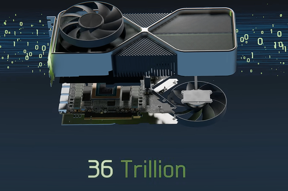
A stylized digital graphic showing a high-end GPU card partially lifted above its printed circuit board. Two large axial fans and a finned heatsink are visible on the card’s shroud, while the PCB below reveals power delivery components and memory modules. Floating binary digits stream in the dark blue background, and the phrase “36 Trillion” appears at the bottom, emphasizing the GPU’s computational throughput.
Fig 2. Modern GPU chassis hovering above its circuit board, illustrating 36 trillion calculations per second

Imagine harnessing every person on Earth, about 8 billion individuals, to each perform a single multiplication per second. Despite this monumental collective effort, you’d reach only around 8 billion operations per second, still a factor of 4,500 below what a single modern GPU can achieve. This staggering gap illustrates why specialized hardware, finely tuned for parallel workloads, is essential.

CPU vs. GPU: Contrasting Design Philosophies

To appreciate why GPUs excel at certain tasks, consider the classic ship-and-plane analogy:

  • CPU (Jumbo Jet): Equipped with a small number of powerful, flexible cores, a CPU handles diverse tasks, running an operating system, managing I/O devices, and executing complex branching code. Its strong single-thread performance is akin to a jet’s speed and versatility, capable of landing at thousands of airports around the globe.
  • GPU (Cargo Ship): Built with thousands of simpler cores, a GPU is optimized for throughput rather than latency. It carries vast quantities of data (graphic primitives, pixel values, matrix elements) in repeatable batches, similar to how a cargo ship transports bulk containers between specialized ports. Loading and unloading cargo may take longer per container than a plane, but the total volume moved per trip is orders of magnitude greater.
FeatureCPU (Jumbo Jet)GPU (Cargo Ship)
Core Count6–24 powerful x86 cores10,000+ CUDA/Cores + hundreds of specialized cores
FlexibilityRuns OS, branching logic, network stacks, diverse applicationsExecutes narrow instruction sets (arithmetic, vector math, shaders)
Throughput vs. LatencyLower throughput, low latency per taskExtremely high throughput, higher per-operation latency
I/O InterfacesDisks, network, USB, keyboard, thousands of connection typesPCIe, NVLink, display ports—high-bandwidth, specialized pathways
Ideal WorkloadsSequential / control-heavy tasks, complex branching, multitaskingEmbarrassingly parallel tasks: 3D rendering, AI training, crypto hashing

By matching hardware design to workload characteristics, GPUs deliver phenomenal performance on data-parallel problems that would bottleneck on a CPU.

Physical Architecture of a Modern GPU (GA102 Example)
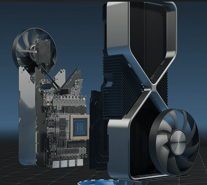
A detailed exploded-render graphic of a high-end GPU (NVIDIA GA102). On the right, the aluminum-and-fin heatsink with dual axial fans is separated from the circuit board. In the center, the green PCB is exposed, showing the large square GPU die surrounded by memory modules and VRM components. On the left, the metal backplate and fan assembly are slightly offset, illustrating the layering of the cooling solution over the circuit board. The dark grid background highlights each component’s position in the assembly.
Fig 3. Exploded view of a modern GA102-based GPU, revealing its heatsink, fans, and PCB components.

Modern GPUs, such as NVIDIA’s GA102 die used in the RTX 30-series, are marvels of semiconductor engineering. Let’s peel back the layers:

Billion-Transistor Die

At the heart of the GPU lies a silicon die spanning just a few square centimeters, yet containing 28.3 billion transistors. These transistors act as digital switches, opening and closing to represent binary 1s and 0s. Without this transistor density, executing trillions of operations per second would remain science fiction.
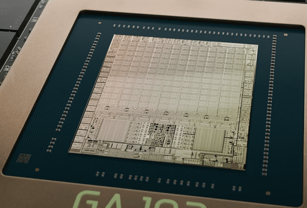
A macro photograph of an exposed GPU silicon die (NVIDIA GA102) mounted on its substrate. The central square die displays a grid of circuit patterns and metal interconnects in gold and silver hues, with fine geometric blocks representing transistor arrays. Around the die’s perimeter are tiny bond pads and solder bumps, all seated within a teal-green package frame.
Fig 4. Close-up of the GA102 GPU’s Silicon die revealing its intricate transistor layout.

Hierarchical Compute Blocks

To organize computation at scale, the die is structured into nested units:

  • Graphics Processing Clusters (GPCs): GA102 features 7 GPCs, each a self-contained block that processes a subset of the rendering workload.
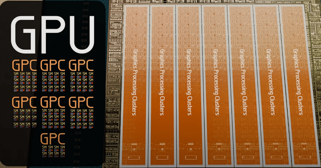
A composite graphic showing the GA102 GPU die segmented into seven vertical blocks, each labeled “Graphics Processing Cluster.” To the left is an overlay illustrating the cluster hierarchy: seven “GPC” labels, each containing icons for Streaming Multiprocessors (SM) within. The background die texture reveals transistor layouts and interconnects, emphasizing how each GPC is a self-contained block handling a portion of the rendering workload.
Fig 5. Diagram of seven Graphics Processing Clusters (GPCs) laid out on the GA102 die.
  • Streaming Multiprocessors (SMs): Each GPC houses 12 SMs, totaling 84 on the GA102. SMs are the workhorses that dispatch and execute threads.
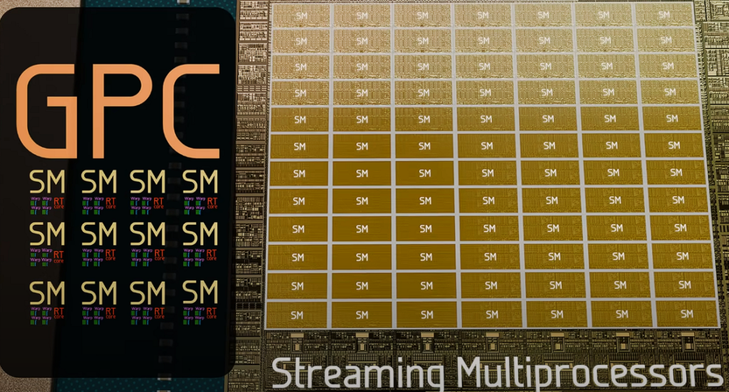
A die-level illustration highlighting the 84 rectangular Streaming Multiprocessor units arranged in a 7×12 grid on the GA102 GPU. To the left, an overlay shows one GPC block subdivided into 12 SM icons, each labeled “SM” with miniature symbols for CUDA, Tensor, and RT cores. The background reveals the underlying transistor metal layers in gold tones, emphasizing the dense array of SM blocks that dispatch and execute parallel threads across the GPU.
Fig 6. Grid view of the 84 Streaming Multiprocessors (SMs) within the GA102’s Graphics Processing Clusters.
  • Warps, CUDA Cores, Tensor & Ray-Tracing Cores:
    • Warp: A group of 32 threads executing the same instruction sequence in parallel.
    • CUDA (Shading) Cores: 32 simple arithmetic units per warp, for a grand total of 10,752 on GA102. They handle basic operations like add, multiply, and bitwise logic, with blazing speed.
    • Tensor Cores: One per warp (336 on GA102), specialized in matrix multiply-accumulate (essential for AI workloads).
    • Ray-Tracing Cores (RT Cores): One per SM (84 total), dedicated to processing ray-tracing acceleration structures and intersection tests.
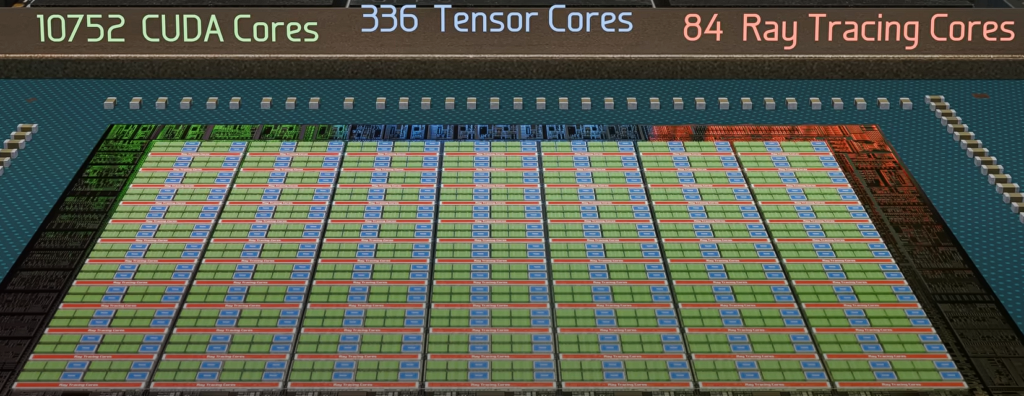
A high-resolution die shot segmented into a grid of small rectangular blocks, overlaid with three colored labels at the top: “10,752 CUDA Cores” in green, “336 Tensor Cores” in blue, and “84 Ray Tracing Cores” in red. The majority of the die area is filled with repeating green-tinted blocks (CUDA cores), interspersed with fewer blue-tinted blocks (Tensor cores) and the rarest red-tinted blocks (RT cores), illustrating the distribution and hierarchy of core types across the GPU’s silicon.
Fig 7. Color-coded layout showing 10,752 CUDA cores alongside 336 Tensor cores and 84 RT cores on the GA102 die.
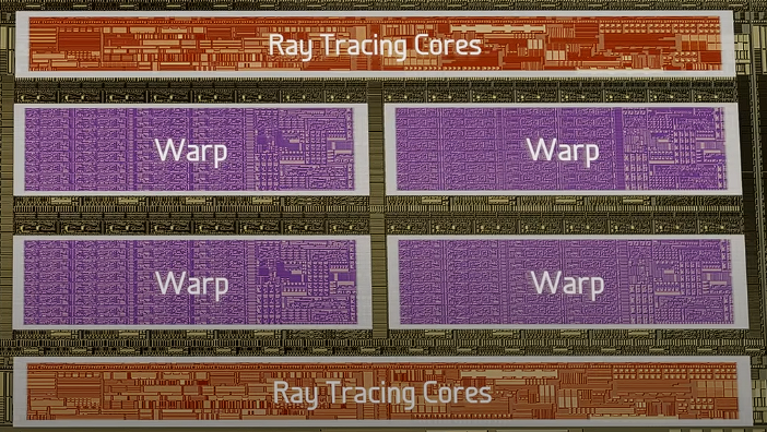
A split illustration: on the left, a golden-hued rectangular block labeled “SM” represents a single Streaming Multiprocessor on the GPU die, with a magnifying-glass graphic highlighting its right edge. An arrow points right to the enlarged interior of that SM, revealing four purple-shaded “Warp” blocks arranged in a 2×2 grid, flanked above and below by orange-shaded “Ray Tracing Cores” blocks. This emphasizes that each SM contains four warps and two dedicated ray-tracing cores.
Fig 8. Zoomed view of one Streaming Multiprocessor (SM) showing its four warp units and two ray-tracing cores.
A close-up die photograph of one GPU Streaming Multiprocessor’s interior. The top and bottom edges feature long, orange-tinted rectangles labeled “Ray Tracing Cores.” Sandwiched between them are four purple-tinted rectangles labeled “Warp,” arranged in two rows of two. Fine transistor patterns and metal interconnects are visible within each block, illustrating how each SM dedicates two ray-tracing cores and four warps of 32 threads each.
Fig 9. Internal layout of a Streaming Multiprocessor showing its four warps flanked by two ray-tracing cores.
A split graphic: on the left, a purple-tinted rectangular block labeled “Warp” represents a single warp unit on the GPU die, with a magnifying-glass icon highlighting its right side. An arrow leads to the right, revealing 32 small green rectangles in four rows of eight, each labeled “CUDA,” and one larger blue rectangle labeled “Tensor” at the end. This illustrates that each warp contains 32 shading cores for arithmetic operations and one dedicated tensor core for matrix math.
Fig 10. Zoomed view of one warp showing its 32 CUDA cores alongside the warp’s single Tensor core.

This hierarchical arrangement ensures work is subdivided and scheduled efficiently, maximizing utilization of the die’s compute resources.

Microscopic View: Inside a CUDA Core
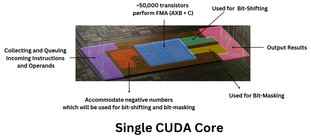
A color-coded microscopic view of one CUDA core’s silicon layout. The central blue rectangle (≈50 000 transistors) is labeled “perform FMA (A×B + C).” To its left, a purple block indicates “Collecting and Queuing Incoming Instructions and Operands.” Below, an orange area “Accommodate negative numbers” feeds into green (“Bit-Shifting”) and yellow (“Bit-Masking”) sections. On the far right, a pink region is labeled “Output Results.” Fine metal interconnects and transistor patterns form the backdrop, illustrating how each core integrates ALUs, sign handling, and control logic.
Fig 11. An annotated microphotograph of a single CUDA core highlighting its internal functional blocks.

A single CUDA core is deceptively complex:

  • Out of ~410,000 transistors present in a single CUDA core, ~50,000 transistors implement a fused-multiply-add (FMA) unit, computing A×B + C in one clock cycle, and additional logic for bit-shifting, masking, and control.
  • Clock Rate & Throughput: At a boost clock of 1.7 GHz, each core achieves 1.7 billion FMAs per second. Multiply that by 10,496 active cores of RTX 3090, and you reach ~35.6 trillion floating-point operations per second (FLOPS).
  • Special Function Units: Four units per SM handle complex operations such as division, square roots, and trigonometric functions that don’t map cleanly to simple FMAs.

Memory Controllers, Caches & I/O

Surrounding the compute clusters are essential support circuits:
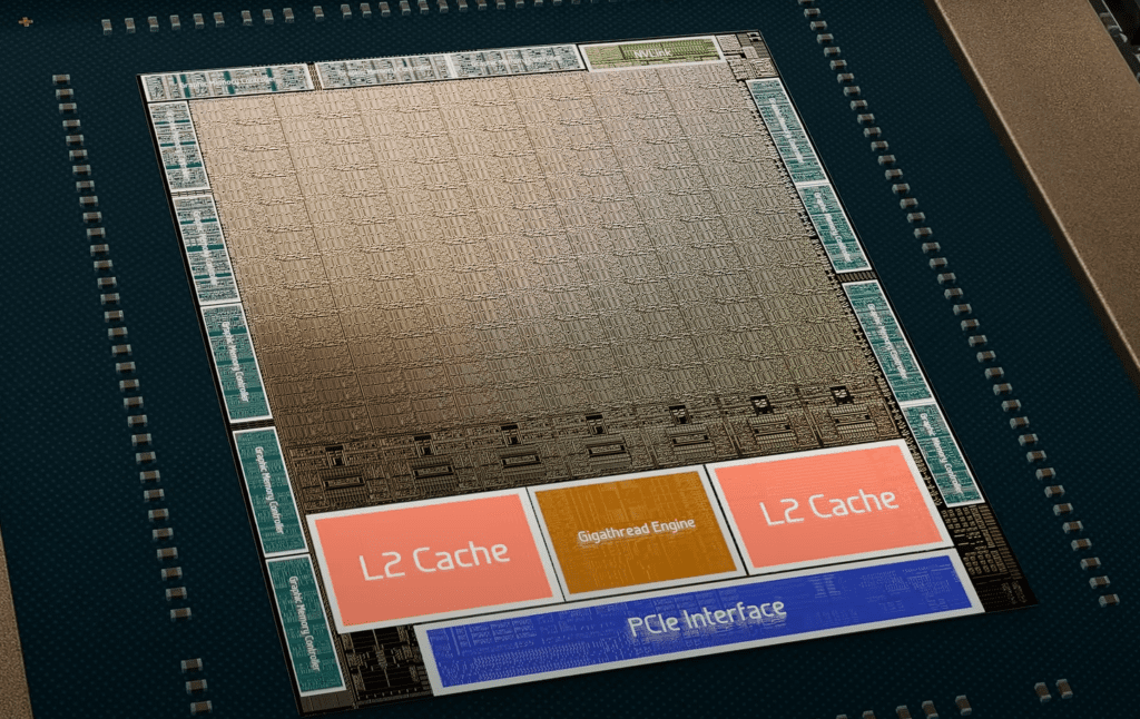
A high-resolution shot of the GA102 GPU die showing the compute clusters above and a row of support circuits below. Two large orange rectangles labeled “L2 Cache” flank an orange “Gigathread Engine” block at the center. Directly beneath them, a blue “PCIe Interface” block spans the width. Surrounding these are teal-tinted memory controller channels (12 total) arrayed along the die edges. The intricate transistor and interconnect patterns in the background illustrate how the GPU’s caches, scheduler, and I/O logic integrate with the main compute clusters.
Fig 12. GA102 die highlighting L2 cache, Gigathread engine, and PCIe interface blocks.
  • Memory Controllers: 12 channels of GDDR6X memory form a 384-bit bus capable of 1.15 TB/s sustained bandwidth.
  • On-Chip Cache: A set of 2 3MB L2 SRAM cache shared across SMs, plus 128 KiB L1 cache per SM, minimizes expensive DRAM round-trips.
  • Gigathread Engine: Manages all 7 Graphics Processing Clusters and Streaming Multiprocessors (SMs) inside.
  • PCIe & NVLink: High-speed serial links connect the GPU to the CPU/motherboard or other GPUs.
  • Display Outputs: 1 HDMI and 3 DisplayPort connectors interface with monitors in real time.
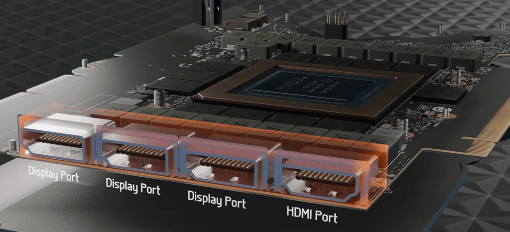
A rendered perspective of the graphics card’s PCB edge highlighting its video outputs. From left to right are three rectangular DisplayPort sockets, each labeled “Display Port,” followed by a slightly wider HDMI port labeled “HDMI Port.” Behind the ports, the PCB’s black substrate is visible along with surface-mounted components and the GPU die. Light reflections on the metal housings emphasize their in-situ placement for real-time video interfacing.
Fig 13. Close-up of a GPU PCB edge showcasing 3 DisplayPort and 1 HDMI connector.

Power Delivery & Thermal Management

Feeding and cooling this beast requires engineering ingenuity:

  • Voltage Regulator Module (VRM): Steps down the 12 V PCIe/auxiliary input to ~1.1 V, delivering hundreds of Watts to the GPU.
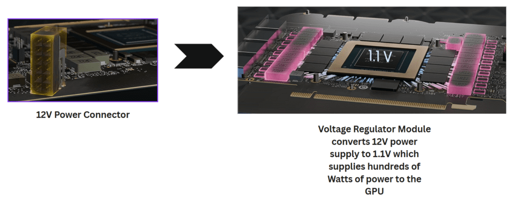
A split rendering: on the left, a translucent yellow-highlighted 12 V auxiliary power connector protrudes from the GPU’s PCB. An arrow points right to the voltage regulator area, where multiple pink-highlighted MOSFETs and inductors flank the GPU die, annotated with “1.1 V.” This illustrates how the VRM circuitry converts the 12 V input into the low-voltage, high-current supply needed by the GPU.
Fig 14. 12 V power input feeding the VRM, which steps the voltage down to ~1.1 V for the GPU.
  • Heatsink & Fans: Massive aluminum fin stacks with copper heat pipes transfer thermal energy to flowing air, kept in check by one or more high-CFM fans.
Two side-by-side renderings of the GPU’s cooling solution. On the left, an orange-highlighted aluminum fin stack labeled “Heat Sink” sits atop the PCB, with a large axial fan visible at one end. On the right, four thick copper heat pipes extend from the GPU die area into the radiator fins, each pipe shaded in gradient pink, illustrating heat transfer toward the fan. The dark patterned floor beneath emphasizes the scale and layering of the thermal module.
Fig 15. Massive GPU heatsink with copper heat pipes and a high-CFM fan assembly.

Binning: One Die, Multiple Products

Instead of discarding dies with minor defects, manufacturers bin them:

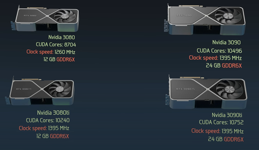
ProductActive CUDA CoresDescription
RTX 3090 Ti10,752Full, defect-free GA102
RTX 309010,496 (2 Defective SMs)Minor disabled SMs post-manufacturing
RTX 3080 Ti10,240 (4 Defective SMs)Additional disabled SMs for mid-tier SKU
RTX 30808,704 (16 Defective SMs)Maximum disabled SMs for entry-level SKU
A graphic showing four NVIDIA RTX 30-series cards and their key specifications arranged in a 2×2 grid. Top left: “Nvidia 3080” with 8 704 CUDA cores, 1 260 MHz clock, and 12 GB GDDR6X. Top right: “Nvidia 3090” with 10 496 CUDA cores, 1 395 MHz clock, and 24 GB GDDR6X. Bottom left: “Nvidia 3080 Ti” with 10 240 CUDA cores, 1 395 MHz clock, and 12 GB GDDR6X. Bottom right: “Nvidia 3090 Ti” with 10 752 CUDA cores, 1 395 MHz clock, and 24 GB GDDR6X. Each card image shows the dual-fan cooler and PCIe edge connector.
Fig 16. Comparison of four GA102-based GPU models with core counts, clock speeds, and VRAM capacities.

Aside from core counts, each SKU varies clock frequencies, VRAM capacity (10–24 GB), and power targets.

Feeding the Beasts: Graphics Memory (GDDR6X, GDDR7, and HBM)

GPUs are data-hungry machines and need a constant data feed to keep thousands of cores busy. The following leading DRAM architectures deliver this:

GDDR6X SDRAM

  • Capacity & Configuration: High-end cards implement 24 chips, each 1 GB, for 24 GB total.
  • PAM-4 Signaling: Transmits 2 bits per pin per clock using four distinct voltage levels, doubling throughput without doubling pin count.
  • Bandwidth: Upwards of 1.15 TB/s on a 384-bit bus.
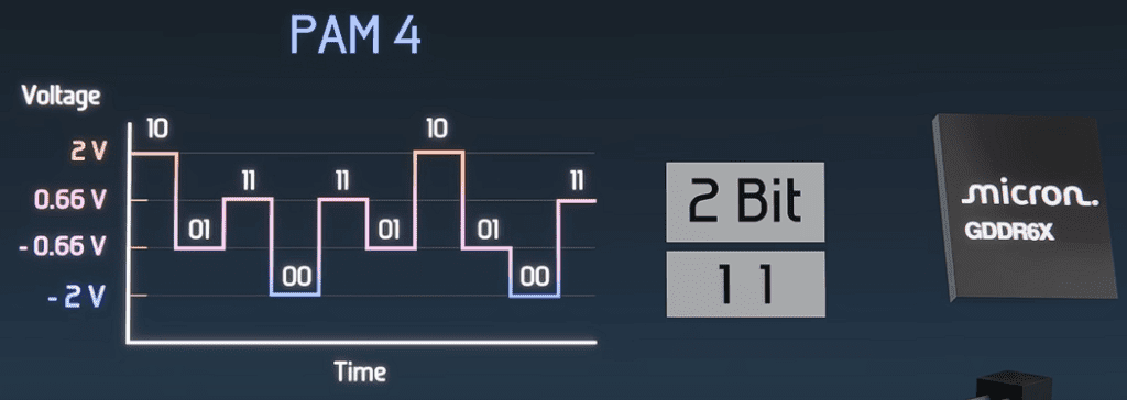
A split graphic featuring on the left a timing diagram labeled “PAM 4,” with voltage on the vertical axis (+2 V, +0.66 V, –0.66 V, –2 V) and time on the horizontal axis. Four distinct voltage steps are marked with binary symbols “10,” “11,” “01,” and “00,” illustrating how two bits are sent per clock using four voltage levels. To the right, a Micron-branded GDDR6X memory chip is shown in 3D, emphasizing its role in high-speed graphics memory.
Fig 17. Signal diagram of PAM-4 showing four voltage levels encoding two bits per cycle

A total of 24 chips transfer combined 384 bits at a time, known as Bus Width. In the CPU, the Bus Width is 64 bits with a bandwidth of 6 GB/sec.

GDDR7 SDRAM

PAM-3 Encoding: Three voltage levels (−1, 0, +1) encode data more efficiently, improving power and signal integrity. GGDR7 uses 3 different encoding schemes to combine binary bits into ternary bits.
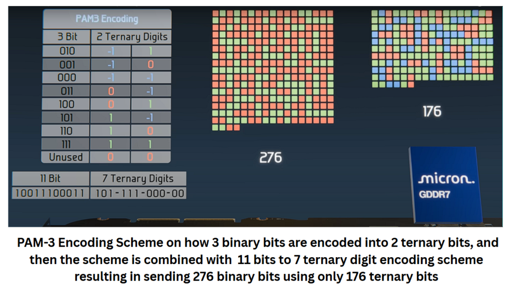
A composite graphic showing how GDDR7’s PAM-3 encoding maps 3-bit binary values into 2 ternary digits (−1, 0, +1). On the left is a table with rows labeled by 3-bit patterns (e.g., 010, 001) and corresponding 2-digit ternary codes color-coded (red for –1, green for 0, blue for +1). Below, an example shows “10011100011” becoming “101 –1 11 –000 –00,” reducing 11 binary bits into 7 ternary digits. To the right are two grids of small colored squares (276 on the left vs. 176 on the right) illustrating the overall bit savings. A Micron GDDR7 chip render sits in the corner, underscoring the memory technology context.
Fig 18. Table and diagram illustrating PAM-3 encoding of binary bits into ternary symbols for GDDR7 efficiency.

High-Bandwidth Memory (HBM3E)

HBM by Micron surrounds AI chips built from stacks of DRAM memory chips and uses TSVs to connect the stack into a single chip.
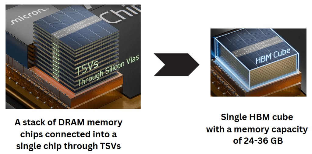
Left: A rendered stack of individual DRAM die sheets on a substrate, with green-highlighted Through-Silicon Vias (TSVs) penetrating the layers, labeled “TSVs Through-Silicon Vias.” Right: The combined “HBM Cube” encased in a translucent outline, noting “24–36 GB” capacity. The background shows a Micron-branded package, illustrating how multiple DRAM chips integrate into one high-capacity memory cube for AI accelerators.
Fig 19. Stacked DRAM chips interconnected by TSVs form a single high-bandwidth memory cube.
  • Stacked DRAM Cubes: Connected via Through-Silicon Vias (TSVs).
  • Capacity & Bandwidth: A single cube can have up to 24–36GB of memory, thus yielding 192 GB/s per stack, which is ideal for AI accelerators.

Parallel Compute Models: From SIMD to SIMT

GPUs excel at embarrassingly parallel tasks, where identical operations are applied independently across vast datasets. Embarrassingly Parallel Workloads are defined by tasks where each data element can be processed independently, whose examples include:

  • 3D vertex transformations
  • Pixel-based image filters
  • Cryptographic hash computations
  • Neural network matrix operations

SIMD (Single Instruction, Multiple Data)

An early model where a single instruction drives a fixed-width vector of data lanes in lock-step, suitable for uniform workloads but inflexible for branching. In simple terms, early GPUs executed one instruction across a fixed set of data lanes, enforcing strict lock-step execution.
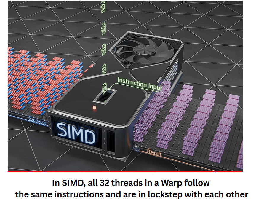
A stylized 3D render of a black box labeled “SIMD” on its front, with red-and-blue square data tiles entering on the left labeled “Data Input.” A green beam labeled “Instruction Input” splits into 32 identical arrows feeding the box’s top. On the right, rows of purple blocks labeled “Result” emerge in perfect alignment, illustrating how all 32 threads in a warp execute the same instruction simultaneously and in lockstep.
Fig 20. Early SIMD model: a single instruction broadcast to all lanes in lockstep.

SIMT (Single Instruction, Multiple Threads)
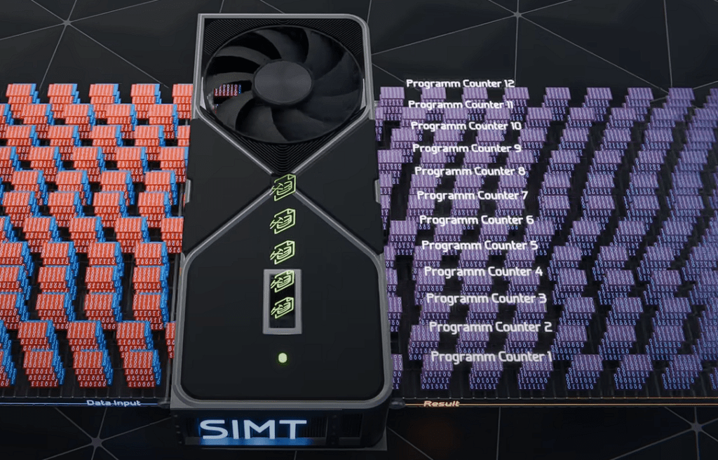
A rendered GPU module labeled “SIMT” on its front. On the left, hundreds of red-and-blue data cubes labeled “Data Input” feed into the box. Above the box, four green arrows labeled “Instruction Input” point down. On the right, rows of purple cubes labeled “Result” emerge, each annotated with “Program Counter 1,” “Program Counter 2,” etc., showing that each thread advances independently. The image illustrates how SIMT allows threads to diverge and reconverge by giving each its own instruction pointer.
Fig 21. SIMT model with each thread maintaining its own program counter for flexible execution.

NVIDIA’s innovation: each thread has its own program counter, enabling:

  • Warp Divergence Handling: Threads in a warp can follow different control paths and later reconverge.
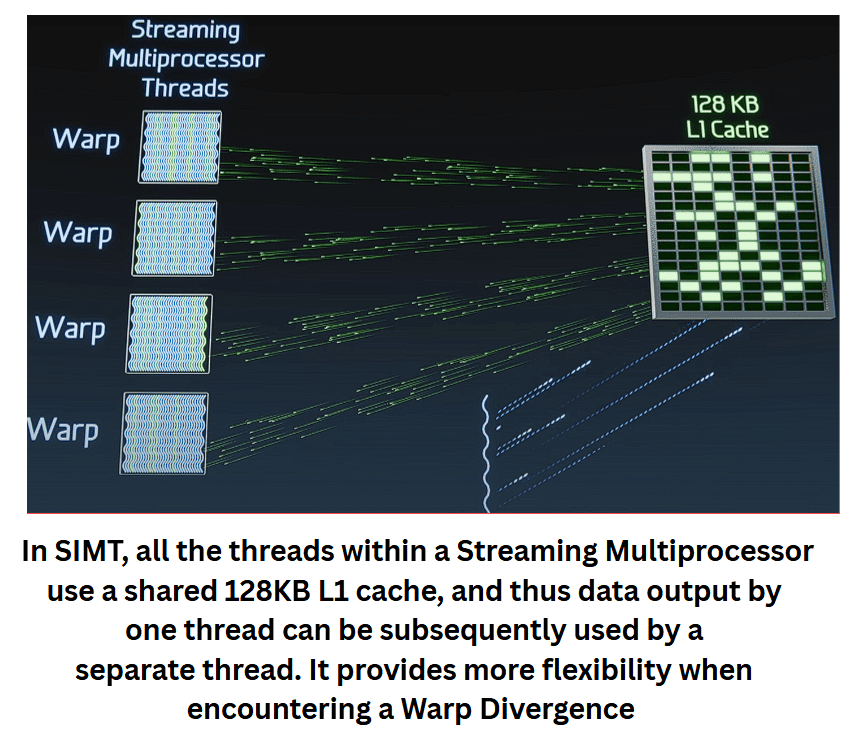
A GPU Streaming Multiprocessor diagram showing four “Warp” blocks on the left, each containing multiple thread icons. Green lines from each warp converge on a shared grid labeled “128 KB L1 Cache,” with white and green cells indicating cached data. To the right, separated blue lines illustrate divergent thread paths that later reconverge. A caption below reads: “In SIMT, all the threads within a Streaming Multiprocessor use a shared 128 KB L1 cache, and thus data output by one thread can be subsequently used by a separate thread. It provides more flexibility when encountering a Warp Divergence.”
Fig 22. Warp divergence in SIMT: threads share an L1 cache yet can diverge and reconverge.
  • Thread Hierarchy Components:
    • Thread: Executes one instruction/data pair on one CUDA core.
    • Warp: 32 threads issuing the same instruction but capable of managed divergence.
    • Thread Block: A collection of warps allocated to one SM.
    • Grid: All thread blocks launched by a GPU kernel.
    • Gigathread Engine: The hardware scheduler that maps blocks to SMs and balances load.

This flexible model empowers developers to write general-purpose GPU code while retaining the massive parallel performance.

Real-World GPU Workloads

3D Graphics Rendering

Consider transforming a cowboy hat model with 14,000 vertices:

  1. Model Space: Vertices relative to the object’s local origin.
  2. World Space Conversion: Add the object’s world-position vector to each vertex coordinate, which is an embarrassingly parallel addition across millions of numerical values.
  3. Pipeline Stages: Rotation, scaling, projection, rasterization, shading—each step parallelized across thousands of fragments or vertices.
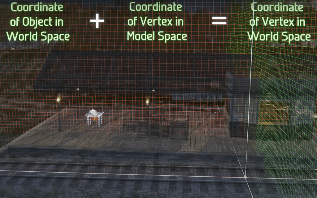
A 3D scene of a train station platform overlaid with wireframe grids. On the left is the text “Coordinate of Object in World Space” above a set of green axes at the object’s location. In the middle, “+ Coordinate of Vertex in Model Space” sits above a close-up of individual wireframe vertices around the object. On the right, “= Coordinate of Vertex in World Space” labels the combined wireframe grid, showing how each vertex’s local coordinates are translated into the shared world-space grid by simple parallel addition.
Fig 23. Vertex transformation: adding an object’s world-position to each model-space vertex.

Cryptocurrency Mining

GPUs previously churned through 95 million SHA-256 hashes per second, trying different nonces in parallel. Modern ASICs now dominate at 250 trillion hashes/sec, showcasing how specialized hardware can eclipse general-purpose GPUs.
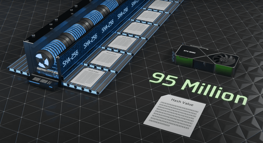
A stylized 3D render on a dark grid floor showing a GPU card (right) labeled “RTX 3090” next to a long rack of blue-and-silver ASIC modules marked “SHA-256.” Beneath the GPU is the text “95 Million” in large green font, and in front lies a printed “Hash Value” slip covered in alphanumeric characters. The contrast highlights that while the GPU achieves 95 million hashes per second, the ASIC rack dwarfs it in throughput.
Fig 24. GPU computing 95 million SHA-256 hashes/sec.

Neural Network Training & Inference (Tensor Cores)

Tensor Cores perform D = A×B + C matrix operations in hardware, enabling:
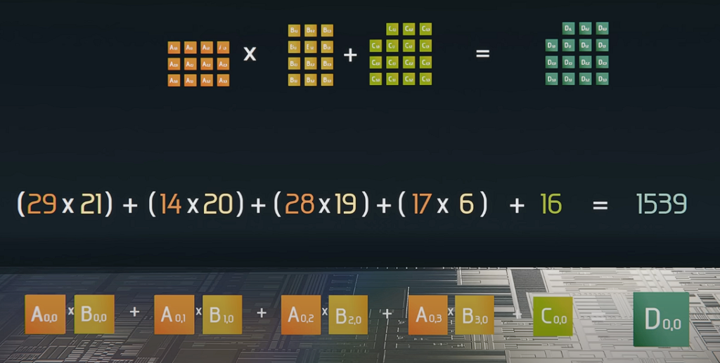
A visual breakdown of a single matrix multiply-accumulate performed by a GPU tensor core. At the top, three small grids represent input matrices A (orange), B (yellow), and C (green), with a larger green grid at right showing the output matrix D. Below, the equation “(29×21) + (14×20) + (28×19) + (17×6) + 16 = 1539” annotates how each element of row 0 and column 0 multiplies and sums with the corresponding element of C₀₀. At the bottom, colored blocks labeled A₀₀, B₀₀, A₀₁, B₁₀, etc., illustrate the individual multiply and add steps that hardware parallelizes to produce D₀₀.
Fig 25. Tensor cores execute a fused matrix multiply-accumulate (D = A×B + C) operation for neural network workloads.
  • Mixed Precision: FP16/INT8 arithmetic to boost throughput while maintaining accuracy.
  • Scale: Trillions to quadrillions of matrix ops per training pass, which is critical for deep learning models like transformers and convolutional networks.

Conclusion

Modern GPUs represent a fusion of semiconductor innovation, parallel computing theory, and practical engineering. From billions of transistors on a silicon die to hierarchical scheduling units and specialized memory technologies, GPUs deliver computational power once reserved for supercomputers. Whether rendering virtual worlds, accelerating AI model training, or simulating scientific phenomena, GPUs continue to redefine the boundaries of what’s possible in computing. As GPU architectures evolve, embracing new memory standards, more flexible parallel models, and even tighter integration with CPUs, the pace of innovation will only accelerate.

References

Read Next

VideoRAG: Redefining Long-Context Video Comprehension

VideoRAG: Redefining Long-Context Video Comprehension

Discover VideoRAG, a framework that fuses graph-based reasoning and multi-modal retrieval to enhance LLMs' ability to understand multi-hour videos efficiently.

AI Agent in Action: Automating Desktop Tasks with VLMs

AI Agent in Action: Automating Desktop Tasks with VLMs

Learn how to build AI agent from scratch using Moondream3 and Gemini. It is a generic task based agent free from…

The Ultimate Guide To VLM Evaluation Metrics, Datasets, And Benchmarks

The Ultimate Guide To VLM Evaluation Metrics, Datasets, And Benchmarks

Get a comprehensive overview of VLM Evaluation Metrics, Benchmarks and various datasets for tasks like VQA, OCR and Image Captioning.

Subscribe to our Newsletter

Subscribe to our email newsletter to get the latest posts delivered right to your email.

Subscribe to receive the download link, receive updates, and be notified of bug fixes

Which email should I send you the download link?


Get Started with OpenCV

Subscribe To Receive

We hate SPAM and promise to keep your email address safe.​