


Today’s post will teach how computer vision impacts the semiconductor industry with a specific example of defect detection and classification.
Introduction
A semiconductor manufacturing process and its design rules are called a technology node, process node, or process technology.
Roughly speaking, the size of a transistor in a 90 nm process technology used by Pentium M in 2003 is nine times larger than a 10 nm process technology used in Icelake processors of 2019. That, in turn, leads to faster speed and lower power consumption.
Scaling of the devices has been happening continuously over the last few decades while keeping Moore’s law alive and valid from node to node, as shown in Fig. 1.

The latest generation semiconductor chips achieve this incredibly small process technology using various techniques like multi-patterning steps or Extreme Ultra-Violet Lithography (EUV).
The final device dimensions are often below 40 nm!
Electron Beam Inspection (EBI)
The quantitative measure of the quality of a semiconductor process is called yield. We can think of it as the ratio of flawless chips that were actually produced to the maximum number of chips that could have been produced.
Extensive inspection and metrology runs are required to ensure a high yield for process technology. Hundreds of process steps must be performed with 99.999% yield to ensure a technology node is profitable!
A semiconductor chip is created in layers, and every layer is scrutinized extensively during the yield ramp to weed out any yield detractors.
Defect detection and analysis need to be as accurate as possible.


While an inspection of these microscopic structures is still possible with optical tools (Broad Band Plasma – ref KLA-Tencor), they still need a lot of Scanning Electron Microscopy (SEM) verification and classification.
The wavelength of electrons is much shorter than the wavelength of photons. Consequently, an Electron Microscope that uses a beam of electrons (e-beam) can resolve finer details. Therefore, measurements done during the design and manufacturing of chips (technically called metrology) require e-beam based tools.
However, metrology using e-beams is inherently noisy, making it difficult to use for correct, repeatable, and accurate measurements.
Fig 1: Scaling in the EUV era [1]

Fig. 2: The Defect Inspection and Review Space
Current state-of-the-art defect detection tools (optical/e-beam) have certain limitations as these tools are driven by some rule-based techniques for defect classification and detection. These limitations often lead to misclassification of defects, which leads to increased engineering time to classify different defect patterns correctly.
This blog post will discuss our proposed deep learning-based approach, based on RetinaNet, to solve challenging defect detection problems in SEM images. In particular, we propose a novel ensemble deep learning-based model to accurately classify, detect and localize different defect categories for aggressive pitches and thin resists (High NA applications).
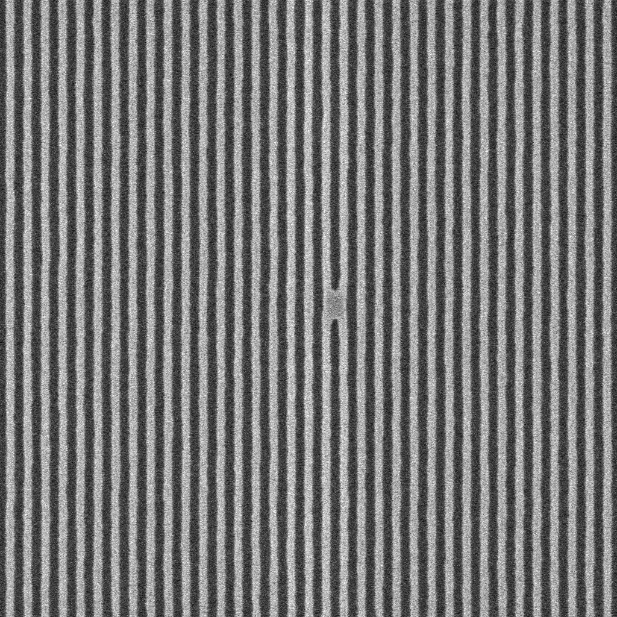
The figure below shows a typical example of a series of lines patterns created by Extreme Ultra Violet Lithography tool (ASML 3400 series scanner) when viewed through a scanning electron microscope (SEM).

Fig. 3: Line-Space pattern
Problems in the patterning process cause defects and should be detected early on and fixed to prevent yield issues and can have disastrous consequences on the final product.
The goal is to detect region-of-interest or defect locations in SEM images. These could be:
- Classification of defect types: bridge, line_collapse, gap/breaks
- Classification in a more challenging scenario: micro-bridges, micro-gaps
- Detection/localization of each distinct defect of interest in the SEM image

(a) (b) (c) (d)
Figure 4: Different defect categories: (a) bridge, (b) line-collapse, (c) gaps/breaks, (d) micro-bridges
The problem is very challenging since these defect patterns are only in the micro/nano-scale range and have varying degrees of pixel-wide defect level. Early detection of these defects helps reduce engineering time and tool cycle time associated with the defect inspection process. Once the defects are correctly detected, different parameters (area, length, width, and additional feature vectors) of the defects can be output for better classification and understanding of the root cause of the defects
1 Proposed Ensemble Model-Based Defect Detection Framework
A. Overview of the RetinaNet architecture
B. Deep feature extractor networks as backbone
2 Experiments
A. Datasets
B. Evaluation criteria
C. Training
3 Running Inference on Test Dataset
4 How Denoising can help in Challenging Defect-Detection Scenario
5 Application
6 Web-based defect inspection app
7 Conclusion
Proposed Ensemble Model-Based Defect Detection Framework
Our proposed ensemble model-based defect detection framework, as illustrated in Fig. 5, consists of the RetinaNet [2] based detector and the U-Net architecture based denoiser [3].
Defect inspection in ADI (After Develop Inspection) SEM images is the most challenging task as different noise sources generally shadow the detailed device feature information. This often leads to false defect detections and erroneous metrology.
The challenge also lies for some resist profiles, in differentiation and detection of minute bridges (micro), breaks (zones of probable breaks), and resist footing from these noisy SEM images. Therefore, we have applied an unsupervised machine learning strategy to denoise the SEM images aiming to optimize the effect of stochastic noise on structured pixels and therefore, to remove the False-Positive defects (FP) for better metrology and enhanced defect inspection. The framework is trained and evaluated using imec datasets (both post-litho and post-etch resist wafer datasets) and classifies, detects, and localizes the candidate defect types.

Fig. 5: Proposed ensemble model-based defect detection framework
The focus of this section is to briefly discuss the key modules of the defect detection network only. The key modules of the defect detection network are:
A. RetinaNet defect detector architecture
B. Deep feature extractor networks as the backbone
A. Overview of the RetinaNet architecture

Fig. 6: RetinaNet defect detector architecture
RetinaNet is a popular one-stage object detection model which works well with dense objects and effectively handles the foreground-background class imbalance problem affecting the performance of other one-stage detector models. RetinaNet architecture consists of a Feature Pyramid Network (FPN) [4] built on top of a deep feature extractor network, followed by two subnetworks, one for object classification and the other for bounding box regression. RetinaNet defect detector architecture is illustrated in Fig. 6.
FPN takes one single resolution input image, subsamples it into multiple lower resolution images, and outputs the feature maps at different scales, thus building a multi-scale feature pyramid representation. Therefore, it enables the detection of objects of varying sizes from different layers of the feature pyramid. FPN combines low resolution features with high-resolution features via a top-down pathway with lateral connections to layers from a bottom-up pathway. The bottom-up pathway generates a feature hierarchy using feature maps of different scales from the input image. The top-down pathway performs up-sampling on the spatially coarser feature maps from higher pyramid levels. The lateral connections are then used to merge the feature maps of the same spatial size from both the paths, which gives semantically strong feature maps.
The classification and regression subnetworks are connected to every layer of the feature pyramid and are independent of each other. The classification subnetwork predicts the probability of an object’s presence for every anchor box and object class. It consists of 4 fully convolutional layers [(3×3) Conv layer with 256 filters and ReLU activation]. It follows another (3×3)convolutional layer having K×A filters where K is the number of classes, and A is the number of anchors (A=9 anchors covering 3 different aspect ratios and 3 different scales).
The regression subnetwork regresses the anchor boxes’ offset against the ground truth object boxes. It is a class-agnostic regressor that does not know what class the objects belong to and uses fewer parameters. The structure is similar to the classification network, except it outputs four bounding box coordinates for every anchor box. Anchor boxes are assigned to ground-truth boxes if the IOU between the boxes exceeds 0.5 and assigned to the background if the IOU is in the range [0,0.4). The anchor boxes having IOU in the range [0.4,0.5) are ignored.
RetinaNet uses focal loss [5], which improves the prediction accuracy giving more importance to the hard samples during training and reducing the contribution of easy samples to the loss. It enhances the cross-entropy loss by introducing a weighting factor to offset the impact of class imbalance and a modulating factor to focus on training the hard negatives and less on the easy examples.
B. Deep feature extractor networks as backbone:
The proposed RetinaNet defect detector framework is an ensemble architecture based on a selective permutation of backbones as ResNet50, ResNet101, and ResNet152, as shown in Fig. 7. TABLE 1 describes custom variants of ResNet architectures with multiple convolutional layers with skip connections across them for feature extraction and fully connected layers for predicting different defect category probabilities. We have taken the affirmative ensemble [6] of the predictions from the 3 ResNet models with preference to the models showing better performance on the test dataset. So, we consider all the predictions from the first model and add predictions from the second-best model that do not overlap with the first model predictions. We use an IOU threshold of 0.5 to consider the boxes as overlapping. In this way, we add the non-overlapping predictions from the third-best model. This ensemble strategy ensures that all the predictions from the three models are taken, improving the accuracy of the test dataset.

Fig. 7: Deep feature extractor networks as the backbone
The goal of our proposed ensemble model-based defect detection framework is based on two significant steps.
In the first step, train a RetinaNet defect detector architecture as discussed above to accurately classify and localize different defect types in SEM images such as bridge, line_collapse, gap, micro-bridges, and micro-gaps, respectively.
In the second step, denoise those SEM images with challenging defects such as micro-bridges and micro-gaps to optimize the effect of stochastic noise on structured pixels. We then reiterate the defect detection step to remove the False-Positive defects (FP) towards better metrology and enhanced defect inspection.
TABLE 1: RESNET50, RESNET101, AND RESNET152 BACKBONE ARCHITECTURE

Experiments
We implemented the ensemble model-based defect detection framework using Keras [7] and Tensorflow [8]. For training, we have used the Keras implementation in [9]. Due to IP (Intellectual property) and data confidentiality reasons, we can not open source our implementation in any form.
Our model has been trained and evaluated on Lambda TensorBook with NVIDIA RTX 2080 MAX-Q GPU.
A. Datasets:
The proposed ensemble model (Classifier + Detector) is trained and evaluated on post-litho, and post-etch P32 (Pitch 32 nm) resist wafer images.
The dataset consists of 5,465 raw SEM images of (1024 ×1024) pixels in TIFF format with stochastic defects such as bridge, line-collapse, gaps/line-breaks, micro/nano-bridges, and probable nano-gaps as well as clean images without any such defects. The representative defect class images from this dataset are already shown in Fig. 4 (a) – (d). We have manually labeled 1170 SEM images 1053 training images, 117 validation images using LabelImg [10] graphical image annotation tool. The defect labeling strategy comprises diverse defect representative and challenging condition instances and as per naming convention in TABLE 2.
The dataset was divided into a training set, a validation set, and a test set, as shown in TABLE 3. We have 2529 defect instances of these five different defect classes for training and 337 instances for validation. To comply with training criteria, we converted all images with “.tiff” format into “.jpg” format. We also implemented different data-augmentation techniques (such as rotation, translation, shearing, scaling, flipping along X-axis and Y-axis, contrast, brightness, hue, and saturation) to balance/increase the diversity of the training dataset defect patterns. We did not consider using any digital twins or synthetic datasets as cited in some previous citations as that does not solve the purpose of tackling real FAB-originated stochastic defectivity scenarios. We have also excluded any fabricated dataset patterned with intentionally placed or programmed defect types.
TABLE 2: DEFECT CLASS LABELING CONVENTION

TABLE 3: DATA DISTRIBUTION OF DEFECT SEM IMAGES

B. Evaluation criteria:
We have considered Intersection over Union (IoU) [11] between the ground truth bounding box and the predicted bounding box ≥ 0.5. The “defect detection confidence score” metric is taken as 0.5. The proposed ensemble model-based defect detector overall performance is evaluated against mAP as Mean Average Precision, where mAP is calculated using the weighted average of precisions among all defect classes. AP or average precision provides the detection precision for one specific defect class. We have also considered the speed of detection per image (average-inference-time in milliseconds). We have taken the affirmative ensemble [6] of the predictions from top k backbones with preference to the models showing better performance on the test dataset. So, we consider all the predictions from the first model and then add those predictions from the second-best model that do not overlap with the first model predictions. We use an IOU threshold of 0.5 to consider the boxes as overlapping. In this way, we add the non-overlapping predictions from the third-best model and so on up to k models. This ensemble strategy ensures that all the predictions from the top k backbones are taken, improving the accuracy of the test dataset. The improvement is noticeable for the most challenging defect category p_gap where the ensemble precision exceeds the individual model precisions.
C. Training
We have first trained the different individual backbone architectures (ResNet50, ResNet101, ResNet152, SSD_MobileNet_v1, SeResNet34, Vgg19, and Vgg16) on our SEM image dataset independently.
For the proposed experiments, we have selected training parameters and hyperparameters as: 40 epochs, batch-size of 1, initial learning rate at 0.00001, learning rate reduction by a factor of 0.1 if learning rate plateaus, and optimizer as ADAM [12]. TABLE 4 provides the comparative analysis for defect detection accuracies obtained per defect class and mAP on test images for the above experimental backbones with a score-threshold 0.5.
We have selected the top three ResNet architectures with 78.7%, 77.5% and 78.8% mean average precision (mAP) respectively and SSD_MobileNet_v1 with 92.5% average precision (AP) for line_collapse defect as our final candidate backbones for the proposed ensemble model framework while discarding the others for worst average precision accuracy per defect class.
The focal loss strategy is implemented for the proposed ensemble model with a weighting factor of α=0.25 and focusing parameter γ=2.0. This helps tackle the class imbalance problem and learn from challenging defect instances.
TABLE 5 presents Test and Validation detection accuracies of top 3 ResNet architecture backbones per defect class along with average inference time in seconds. The proposed RetinaNet framework is an ensemble architecture based on a selective permutation of backbones as ResNet50ResNet152ResNet101. As presented in TABLE 6, our proposed ensemble approach achieves better results with an overall mAP of 81.6% than the results obtained by the 3 top individual backbones separately, as shown in TABLE 4. There is further scope to improve the overall mAP metric by ensembling SSD_MobileNet_v1 architecture as a backbone with 92.5% average precision (AP) for line_collapse defect.
TABLE 4: IMPLEMENTATION RESULTS WHEN EXPERIMENTING WITH DIFFERENT BACKBONE ARCHITECTURES

TABLE 5: TEST/VALIDATION ACCURACY OF TOP 3 RESNET ARCHITECTURE BACKBONES

TABLE 6: OVERALL TEST ACCURACY OF PROPOSED RETINANET [ENSEMBLE_RESNET] FRAMEWORK
![OVERALL TEST ACCURACY OF PROPOSED RETINANET [ENSEMBLE_RESNET] FRAMEWORK](https://learnopencv.com/wp-content/uploads/2022/01/OVERALL-TEST-ACCURACY-OF-PROPOSED-RETINANET-ENSEMBLE_RESNET-FRAMEWORK.jpg "OVERALL-TEST-ACCURACY-OF-PROPOSED-RETINANET-ENSEMBLE_RESNET-FRAMEWORK – LearnOpenCV")
Running Inference on Test Dataset
Let’s now look at some results where the RetinaNet-inspired model could identify e-beam defects correctly. Fig. 8, Fig. 9, and Fig 10 show multiple defects of bridge, line-collapse, and gap/line-break categories, respectively. Fig. 11 shows the robustness of our proposed model in detecting relatively few, more challenging probable nano-gap defects in the presence of frequent gap defectivity. Differentiating these two marginal defect categories is challenging for current tools that use rule-based approaches. However, our proposed model demonstrates (1) semantic segmentation between two distinct defect classes as (a) gap/line-break and (b) probable nano-gap and (2) instance segmentation as detection of each distinct defect of interest under these two defect classes in the same image.
Domain experts reported that when image intensity varies strongly from one line in the image to another, the performance in conventional tools takes a hit [13]. This contrast change may be caused due to different levels of charging when a line, sometimes outside the current field of view, is broken. Fig. 12 and Fig. 13 show that our proposed model can classify and detect the above-mentioned two marginal defect categories.
Fig. 14 and Fig. 15 show detection results of more challenging nano-bridge/micro-bridge defectivity on the test image dataset. The test image dataset was used to validate the proposed model performance and robustness as it is unseen during training and of a different resist family. The composition of a resist is a significant variable that impacts the number of stochastic defects like microbridge and possible nano-gap defects. The proposed model demonstrates robustness in detecting individual micro-bridges regardless of their extent. Our proposed ensemble model-based defect detection framework achieves the detection precision (AP) of 95.9% for gap, 86.7% for bridge, 82.8% for line_collapse, 67.5% for microbridge, and 52.0% for probable nano-gap defectivity, respectively. However, we believe there is a scope for further improvement for average precision for specific classes like microbridge and probable nano-ga in the future.

Fig. 8: Multiple correctly identified defects of bridges.

Fig. 9: Multiple correctly identified defects of line-collapses.

Fig. 10: Multiple correctly identified defects of gaps.

Fig. 11: Detection results of more challenging probable nano-gap separately in the presence of gaps. The model shows robustness in detecting relatively few probable nano-gap defects in the presence of frequent gap defectivity.

Fig. 12: Detection of nano-gap (green) and probable nano-gap (yellow) in the presence of contrast change. Contrast change does not affect the defect detection performance of the proposed ML model compared to the conventional approach.

Fig. 13: Detection of nano-gaps in the presence of contrast change. Contrast change does not affect dthe efect detection performance of the proposed ML model compared to the conventional approach.

Fig. 14: Detection results on more challenging nano-bridge/micro-bridge defects.

Fig. 15: Detection results of more challenging nano-bridge/micro-bridge defects on new TEST dataset. The model demonstrates robustness in detecting variable degrees of pixel-level micro-bridge defectivity.
How Denoising can help in Challenging Defect-Detection Scenario

Fig. 16: Defect detection on same Noisy SEM image [P32] with micro/nano-bridges: (a) Conventional Tool/approach, (b) Proposed ensemble model based approach

Fig. 17: Defect detection on same Denoised SEM image [P32] with micro/nano-bridges: (a) Conventional Tool/approach, (b) Proposed ensemble model-based approach
In this section, we have demonstrated how denoising can improve defect inspection performance and accuracy in challenging defect-detection scenarios, specifically in the case of micro-bridge detection. The extraction of repeatable and accurate defect locations and CD metrology becomes significantly complicated in ADI SEM images due to continuous shrinkage of circuit patterns (pitches less than 32 nm). The noise level of SEM images may lead to false defect detections and erroneous metrology. Hence, reducing noise in SEM images is of utmost importance. In the presence of stochastic noise on structured pixels, resist footing generally appears as tiny microbridges that are expected to be removed during the next etch process step. Denoising optimizes this effect of stochastic noise on structured pixels and, therefore, helps to remove the false-positive defects (FP) for better metrology and enhanced defect inspection. We have shown two different strategies in this research as (1) remove any FP detection with strict defect detection confidence score ≥ 0.5 for microbridge and (2) adaptation of resist footing as “weak microbridge” defect by lowering the confidence score enough (0.0 ≤ score ≤0.5). In Fig. 16 and Fig. 17, we have presented both approaches. For the first approach, we have repeated the defect inspection step on denoised images with the same trained model parameters with noisy images only, whereas for the later, we have retrained the model with denoised images and fine-tuned the model parameters. Another approach is possible as labeling of resist footing as a new defect category and training the model. This will be considered as our future scope of this research.
Moreover, we have presented a comparative analysis on stochastic defect detection performance between our proposed deep learning-based approach and conventional approach [13]. Fig. 16 provides a challenging micro/nano-bridges detection scenario on the same Noisy L/S SEM image. With a “manual” selection of the detection threshold parameters (such as user-defined intensity-threshold, failure size parameter, noise etc.), the conventional approach was able to flag four out of seven observable defects. Whereas, our proposed deep learning based model automatically detects five out of the same with a strict defect detection confidence score ≥ 0.5 without any requirement of such manual trial-and-error based “threshold” selection method. Lowering the automated “confidence score” certainly flags other missing defects as demonstrated in Fig. 17. Fig. 17 demonstrates the same challenging micro/nano-bridges detection scenario on the corresponding denoised image. We can see the detection scenario is influenced by the condition if the image is noisy or denoised for conventional approach. Furthermore, after denoising, along with previous undetected defect instances, the conventional approach was not able to detect the “most obvious” microbridge defect instance which was flagged before. However, our proposed model demonstrates “stable” performance in detecting defects with better accuracy for both noisy or denoised images and replaces the manual trial-and-error based “threshold” selection method with automated “confidence score”. Once defects are correctly detected, different parameters (as length, width, area, additional feature vectors) about the defects can be output for better understanding the root cause of the defects.
Application
Web-based defect inspection app

Fig. 18: Web-based defect inspection app
We built a UI (User-Interface) using the Streamlit library in python script to deploy our proposed model as a web-based defect inspection app. A view of the application interface is depicted in Fig. 18. This is a template version of the originally proposed software interface, and we will add more user-friendly graphical widgets in near future. This will enable different partners/vendors to run the application on their local servers/workstations on their own tool data. This UI will enable the users to upload a dataset of SEM/EDR/Review-SEM images, to select and run one out of different defect detection inference models on the dataset, to visualize the prediction performance locally and finally to segregate and save the images in different folders according to their defect categorical classes in local machines.
Conclusion
In this post, we have presented a novel, robust, supervised deep learning training scheme based on RetinaNet architecture to accurately detect different defects in SEM images in aggressive pitches. This scheme includes:
- Classification of defect types: bridge, line-collapse, line-breaks
- Classification in more challenging scenario: micro-bridges, micro-gaps
- Detection/Localization of each distinct defect of interest in the SEM image
We have also investigated and demonstrated how the condition influences defect detection scenarios if the image is noisy or denoised and how denoised SEM images are aiding for better metrology and enhanced defect inspection. Future research direction can be extended to use data to model defect transfer from litho to etch as well as to other SEM applications (Logic/CH structures) as well as use TEM/AFM images.
References:
- C. Zahlten, P. Gräupner, J. van Schoot, P. Kürz, J. Stoeldraijer, W. Kaiser, “High-NA EUV lithography: pushing the limits,” Proc. SPIE 11177, 35th European Mask and Lithography Conference (EMLC 2019), 111770B (29 August 2019); https://doi.org/10.1117/12.2536469
- T.-Y. Lin, P. Goyal, R. Girshick, et al., “Focal loss for dense object detection,” in 2017 IEEE International Conference on Computer Vision (ICCV), 2999–3007 (2017).
- B. Dey, S. Halder, K. Khalil, et al., “SEM image denoising with unsupervised machine learning for better defect inspection and metrology,” in Metrology, Inspection, and Process Control for Semiconductor Manufacturing XXXV, O. Adan and J. C. Robinson, Eds., 11611, 245 – 254, International Society for Optics and Photonics, SPIE (2021).
- T.-Y. Lin, P. Dolla´r, R. Girshick, et al., “Feature pyramid networks for object detection,” (2017).
- T.-Y. Lin, P. Goyal, R. Girshick, et al., “Focal loss for dense object detection,” in 2017 IEEE International Conference on Computer Vision (ICCV), 2999–3007 (2017).
- A. Casado-Garc´ıa and J. Heras, “Ensemble methods for object detection,” (2019). https: //github.com/ancasag/ensembleObjectDetection.
- F. Chollet et al., “Keras,” (2015).
- M. Abadi, A. Agarwal, P. Barham, et al., “TensorFlow: Large-scale machine learning on heterogeneous systems,” (2015). Software available from tensorflow.org.
- https://github.com/fizyr/keras-retinanet
- I. Lu¨tkebohle, “LabelImg.” https://github.com/tzutalin/labelImg (2015).
- H. Rezatofighi, N. Tsoi, J. Gwak, et al., “Generalized intersection over union: A metric and a loss for bounding box regression,” in 2019 IEEE/CVF Conference on Computer Vision and Pattern Recognition (CVPR), 658–666 (2019).
- D. P. Kingma and J. Ba, “Adam: A method for stochastic optimization,” (2017).
- P. D. Bisschop, “Stochastic printing failures in extreme ultraviolet lithography,” Journal of Micro/Nanolithography, MEMS, and MOEMS 17(4), 1 – 23 (2018).


100K+ Learners
Join Free OpenCV Bootcamp3 Hours of Learning